Is Making Chips Smaller Still Enough?
For decades, the semiconductor industry’s formula for success was to make transistors smaller and improve PPAC (Power, Performance, Area, Cost).* The industry evolved toward higher performance, lower power consumption, and more functionality at lower cost. Moore’s Law symbolizes this long standing trend.
As scaling progressed, however, physical limitations and manufacturing costs increased, making it increasingly difficult to improve performance through conventional approaches alone. To overcome these challenges, transistor structures evolved from planar designs to increasingly three dimensional architectures such as FinFET and GAA. New materials and process technologies were also introduced to sustain the benefits of scaling.
These developments gave rise to the More Moore strategy, which extends the benefits of scaling through advances in transistor structures, materials, and processes, and the More than Moore strategy, which integrates different functions and technologies to increase the value of the overall system.
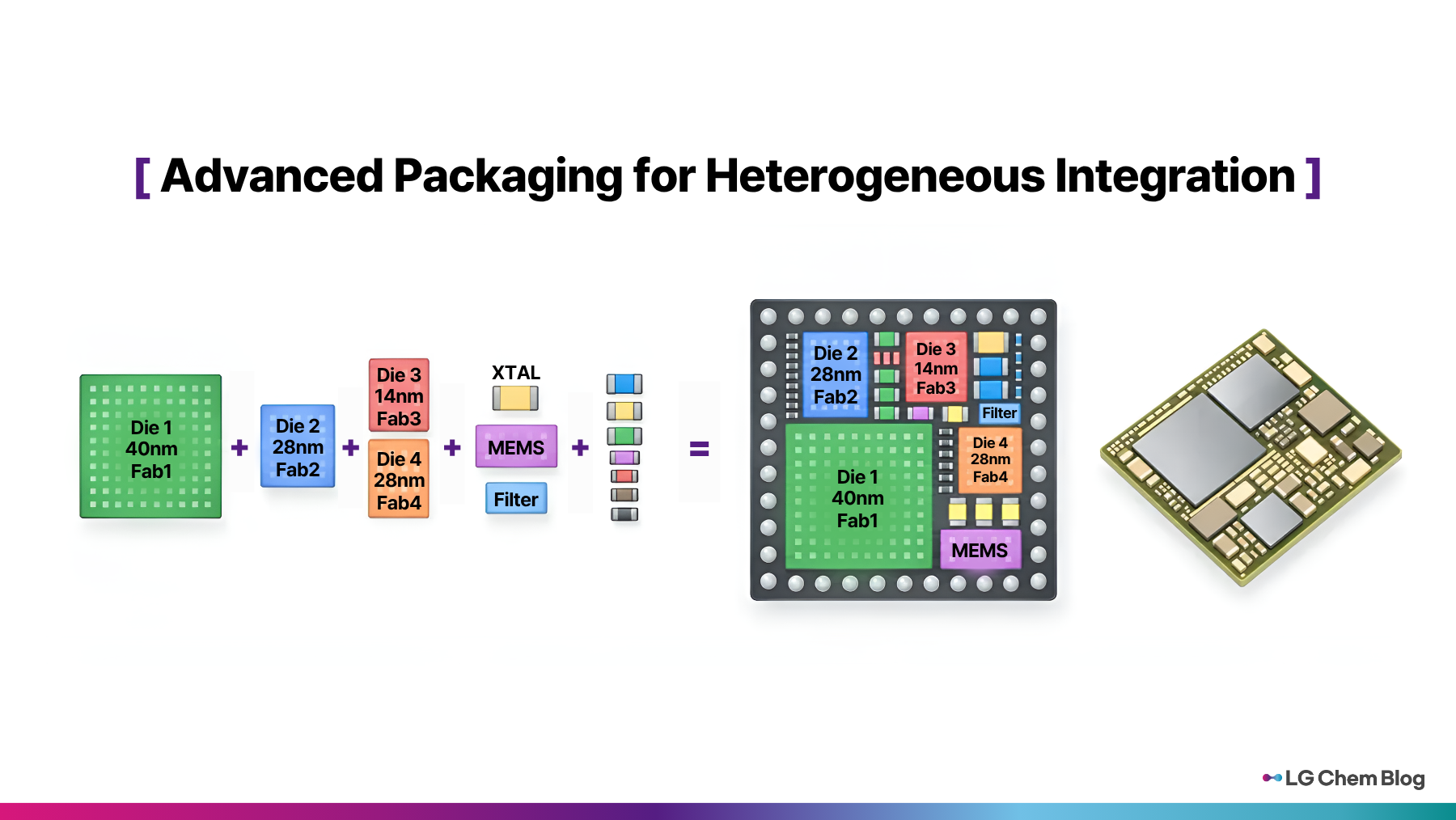
More recently, heterogeneous integration technologies such as chiplets,* HBM, 3D stacking, and advanced packaging have become increasingly important. System connectivity technologies such as CXL* and approaches such as STCO* have also become familiar terms in the semiconductor industry.
* PPAC: The four key metrics used to evaluate semiconductors: Power, Performance, Area, and Cost.
* Chiplet: A technology that divides the functions of one large chip into smaller chips, manufactures each using a process optimized for its specific function, and then integrates them into a single package.
* CXL (Compute Express Link): A next generation interface technology that connects devices such as CPUs, GPUs, and memory more quickly and efficiently.
* STCO (System Technology Co Optimization): An approach that designs and optimizes semiconductor devices and processes from the perspective of the final system, including software, packages, and boards, rather than focusing only on individual chips.
The AI era is now driving another shift. The scope of semiconductor competition is expanding beyond individual transistors and chips to racks connecting dozens of GPUs and even data centers running thousands of accelerators.
In the past, the industry largely followed a bottom up approach, improving transistor performance first and then using those advances to build better systems. Today, however, the importance of a top down approach is growing. The performance requirements and targets of the final system are defined first and then reflected in chip, process, and material technologies.
This means that targets for packaging, interconnects, materials, power delivery, and thermal management are increasingly being set according to system level requirements. Materials and equipment suppliers must also develop technologies that meet these system requirements.
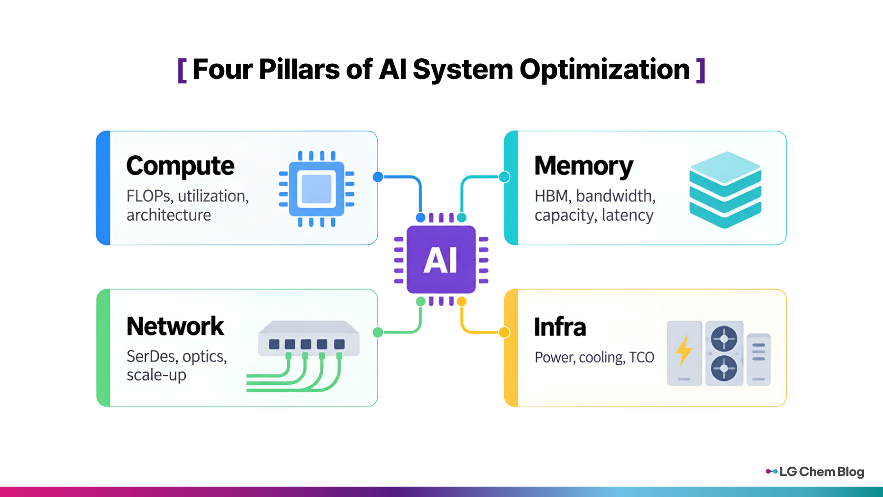
The goal remains the same: to perform more computation at the same cost and power consumption. But the means of achieving that goal are expanding from scaling, architecture, and 3D integration to broader system co-design that includes networking, power delivery, cooling, and infrastructure.
What Does AI Demand from Semiconductors?
AI is changing how semiconductor competitiveness is evaluated. Computing speed alone is no longer enough. Throughput per watt, memory bandwidth, data travel distance, communication latency, and cooling capacity are all becoming important performance factors.
The technical bottlenecks facing semiconductors in the AI era can be broadly grouped into three areas.
The first is memory bandwidth and data delivery.
AI models perform massive amounts of matrix computation. Even with powerful GPUs, high performance processors can remain idle if the data they need is not supplied at the right time. To address this issue, high bandwidth memory, or HBM, is placed close to GPUs to reduce the time and energy required to move data.
The second is data communication within and between systems.
As AI models grow larger, a single GPU or server can no longer handle all the required computation. Multiple GPUs must exchange data and work on the same task in parallel. In this environment, communication bandwidth and latency between GPUs can limit overall system performance.
To address this issue, high speed electrical interconnect technologies such as NVLink* continue to advance, while optical interconnect technologies are also expected to play an important role in the future. One example is the CPO (Co Packaged Optics) technology roadmap presented by SK hynix and researchers from around the world in August 2026. The goal is to improve bandwidth and energy efficiency by shortening the distance traveled by high speed electrical signals and converting some communication links to optical connections.
* NVLink: A high speed chip to chip interconnect technology developed by NVIDIA to enable rapid data exchange.
The third is power delivery and heat generation.
NVIDIA’s GB200 NVL72 integrates 72 GPUs and 36 CPUs in a single rack. The system is a high density computing architecture that consumes approximately 120 kW of power, giving it a much higher power density than conventional server racks. As a result, major heat generating components such as GPUs and CPUs use direct liquid cooling instead of conventional air cooling.
Power consumption across entire data centers is also rising rapidly.
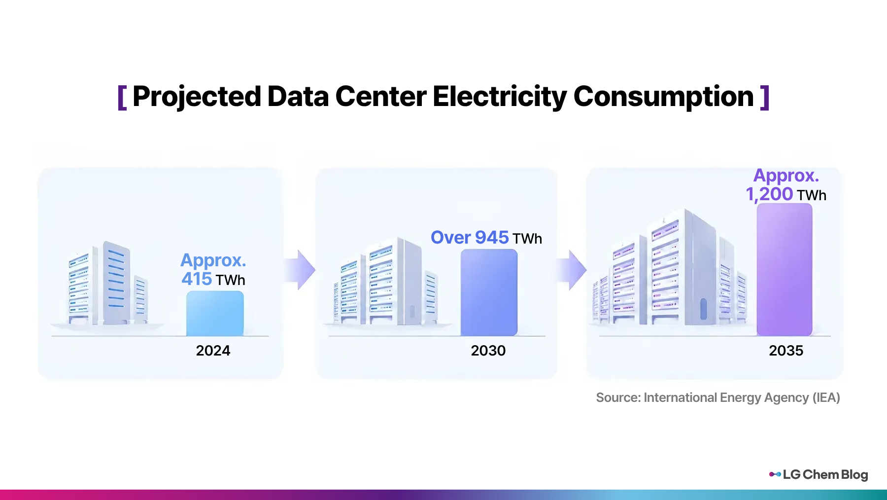
The International Energy Agency (IEA) projects that global data center electricity consumption will increase from approximately 415 TWh in 2024 to around 945 TWh in 2030, reaching approximately 1,200 TWh by 2035. This means electricity consumption could more than double in just six years.
For AI systems, improving computing performance alone is therefore not enough. It is also important to reduce the energy required to move data, deliver power efficiently, and remove generated heat effectively.
Going forward, the competitiveness of AI semiconductors is expected to increasingly depend on how little power is needed to produce the same AI result. This means that energy efficiency will become a competition spanning semiconductor devices, memory, packages, and data center cooling.
Where Is the Next Battleground?
To address these challenges, advanced packaging and 3D stacking are emerging as increasingly important technologies.
In addition to conventional single chip integration, heterogeneous integration is becoming more important. This approach integrates logic, memory, and I/O chiplets manufactured using processes optimized for each function into a single package. Key technologies used to connect these chiplets include TSVs,* microbumps, and hybrid bonding.*
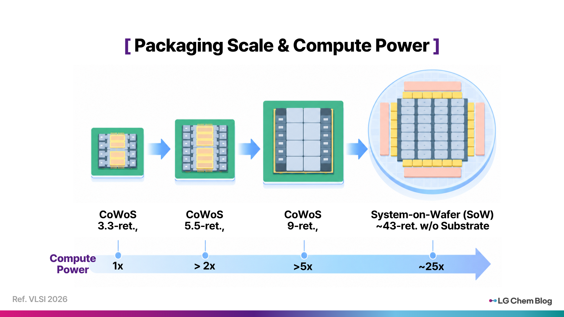
A representative example is TSMC’s CoWoS (Chip on Wafer on Substrate) technology. CoWoS is an advanced packaging technology that connects GPUs and multiple HBM stacks through high density interconnects based on an interposer.*
CoWoS-S uses a large silicon interposer, while CoWoS-L combines redistribution layers (RDL) with localized silicon interconnect structures, enabling expansion to larger package sizes. CoWoS-L has already been in mass production at 3.5 times the reticle* size since 2024, while technologies for larger 5.5 times and 9.5 times reticle sizes are under development.
This shows that the practical unit of integration for advanced AI semiconductors is expanding from a single die to a much larger package that connects multiple dies.
* TSV (Through Silicon Via): A technology that creates microscopic holes through a chip and directly connects vertically stacked chips using electrodes. Compared with conventional wire connections, TSVs enable faster data transfer and lower power consumption.
* Hybrid Bonding: A technology that stacks chips by directly bonding copper to copper without conventional bumps, or microscopic solder balls.
* Interposer: An intermediate substrate that connects fine circuits between different chips, such as GPUs and HBM.
* Reticle Size: The maximum circuit area that semiconductor lithography equipment can expose in a single exposure
As Scaling and Packaging Advance, Materials Become More Important
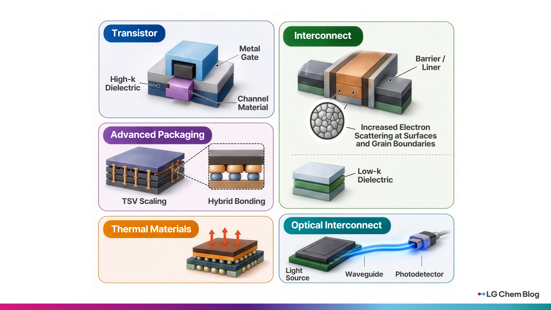
As semiconductor scaling progresses, performance improvements become increasingly difficult to achieve through dimensional reduction alone. The physical properties of materials and the ability to control interfaces are becoming increasingly important. In transistors, research continues into new channel materials. At the same time, further improvements are needed in high k gate dielectrics and metal gates to suppress gate leakage current.
The challenges are even greater in interconnects. As copper interconnects become narrower, electron scattering increases at surfaces and grain boundaries. At the same time, barriers and liners occupy a larger share of the available space, increasing interconnect resistance and delay.
To address these challenges, new barrier, liner, and metal materials, as well as selective deposition technologies, are being developed. Notably, new metals such as molybdenum (Mo) are being actively studied to overcome the limitations of tungsten (W) contacts, which have traditionally been widely used. Low k dielectric materials are also becoming increasingly important for reducing capacitance between interconnects.
In advanced packaging, TSVs and bonding interfaces are also being scaled down to increase chip to chip connection density. The International Roadmap for Devices and Systems (IRDS) projects that TSV spacing will continue to decrease through 2030. Hybrid bonding is also gaining attention as a way to overcome the limitations of microbumps in die to die connections. Hybrid bonding directly joins copper and insulating layers without using conventional solder bumps, enabling high connection density and shorter data travel paths. At the same time, challenges related to crosstalk, warpage, stress, localized heat buildup, and manufacturing costs are expected to increase as scaling advances.
As the power density of AI systems rises, thermal management materials are also becoming more important. To effectively transfer heat generated inside semiconductors to the outside, materials such as TIMs (Thermal Interface Materials), encapsulation materials, and bonding materials with excellent thermal conductivity are required. In vertically stacked structures such as HBM, controlling both thermal resistance and mechanical stress is particularly important.
For this reason, materials must be evaluated not only for thermal conductivity, but also for their coefficient of thermal expansion, adhesion properties, and long term reliability. The growing importance of high speed communication in AI systems is also creating new opportunities for materials used in optical interconnect technologies. Technologies such as CPO require optical waveguides, photodetectors, and light sources to be integrated with semiconductor packages, creating demand for new optical materials and precision bonding technologies.
These changes show that the role of materials technology is expanding beyond conventional devices and interconnects into power delivery, thermal management, and optical communications.
Korea has built strong competitiveness in memory technologies such as DRAM and HBM. If this strength can be extended into advanced packaging and materials technologies, Korea could play an even more important role in the AI semiconductor ecosystem.
The Korean government is also pursuing a support program in 2026 to establish infrastructure for the demonstration and evaluation of advanced semiconductor packaging technologies.
Amid these changes, semiconductor materials companies must go beyond simply understanding customers’ next generation product roadmaps. They must anticipate the technical limitations customers are likely to face and proactively develop the materials and process technologies needed to overcome them.
It will be increasingly important to build distinctive technological capabilities that are difficult to replace. The scope of competition in the semiconductor industry is expanding from chips to systems, but one of the key drivers for overcoming new technological limits remains materials innovation.
About the Author
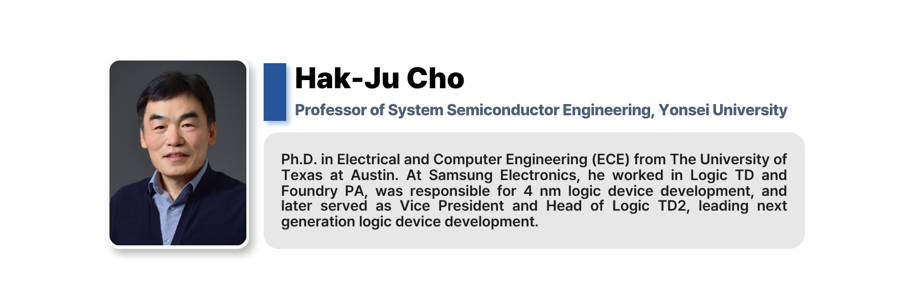
LG Chem Semiconductor Materials Insight Series
This series shares in depth knowledge and insights from LG Chem together with experts and opinion leaders in the field of semiconductor materials.
From changes in the semiconductor industry brought about by the AI era to advanced packaging technologies, next generation core materials, and the outlook for the future industrial ecosystem, the series will explore key developments shaping the semiconductor industry.
[🔍 More from the “Semiconductors Through Materials” Series]
Part 1) Why We Need to Look at the Semiconductors Behind AI
Part 2) How Is AI Reshaping the Semiconductor Industry?
※ Some images in this content were generated using AI





There are no comments yet! Be the first to let us know your thoughts!