How Did NVIDIA Become a Global Leader Without Its Own Chip Factories?
NVIDIA does not operate its own semiconductor factories. It is what the industry calls a fabless company, meaning it specializes in chip design. Think of it as an architect who designs a building rather than constructing it. NVIDIA started as a graphics chip company in 1993, but has since evolved into a computing platform company that provides not only graphics processing units (GPUs), but also CUDA, networking technologies, and system solutions. CUDA is software that makes it easier for developers to use NVIDIA GPUs.
This is why NVIDIA’s competitive strength cannot be explained by its GPUs alone. In the AI era, chip performance is only part of the equation. Software that makes chips easier for developers to use, along with the ability to connect multiple chips into a single system, has also become a key competitive advantage.
TSMC, by contrast, took a different path. Rather than designing the building itself, TSMC is more like a construction company that takes a blueprint and turns it into a finished structure. Instead of developing its own chip products and competing with its customers, TSMC built its business around the pure-play foundry model, manufacturing chips designed by other companies.
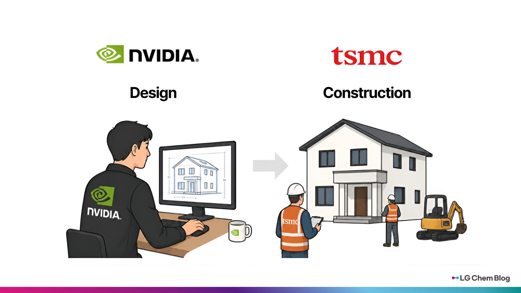
The division of labor between fabless companies and foundries is not new to the AI era. However, as AI chips become more complex and the investment required for advanced manufacturing processes grows, the advantages of this model are becoming even more apparent. Fabless companies can focus on developing new chip architectures and designs without owning massive manufacturing facilities, while foundries can build manufacturing expertise and process know-how by producing chips for a wide range of customers. This specialization in design and manufacturing has helped shape the vast semiconductor ecosystem we see today.
AI is further reinforcing this division of labor.
Why Are Google and Amazon Designing Their Own Chips?
In the past, semiconductor companies such as Intel, AMD, and NVIDIA typically developed chips, while technology companies like Google and Amazon purchased and used them. But in the AI era, the line between these two industries is becoming less clear. Google is designing its own TPUs, Amazon its Trainium and Inferentia chips, and Meta its MTIA chips, all tailored to their AI services and data centers.
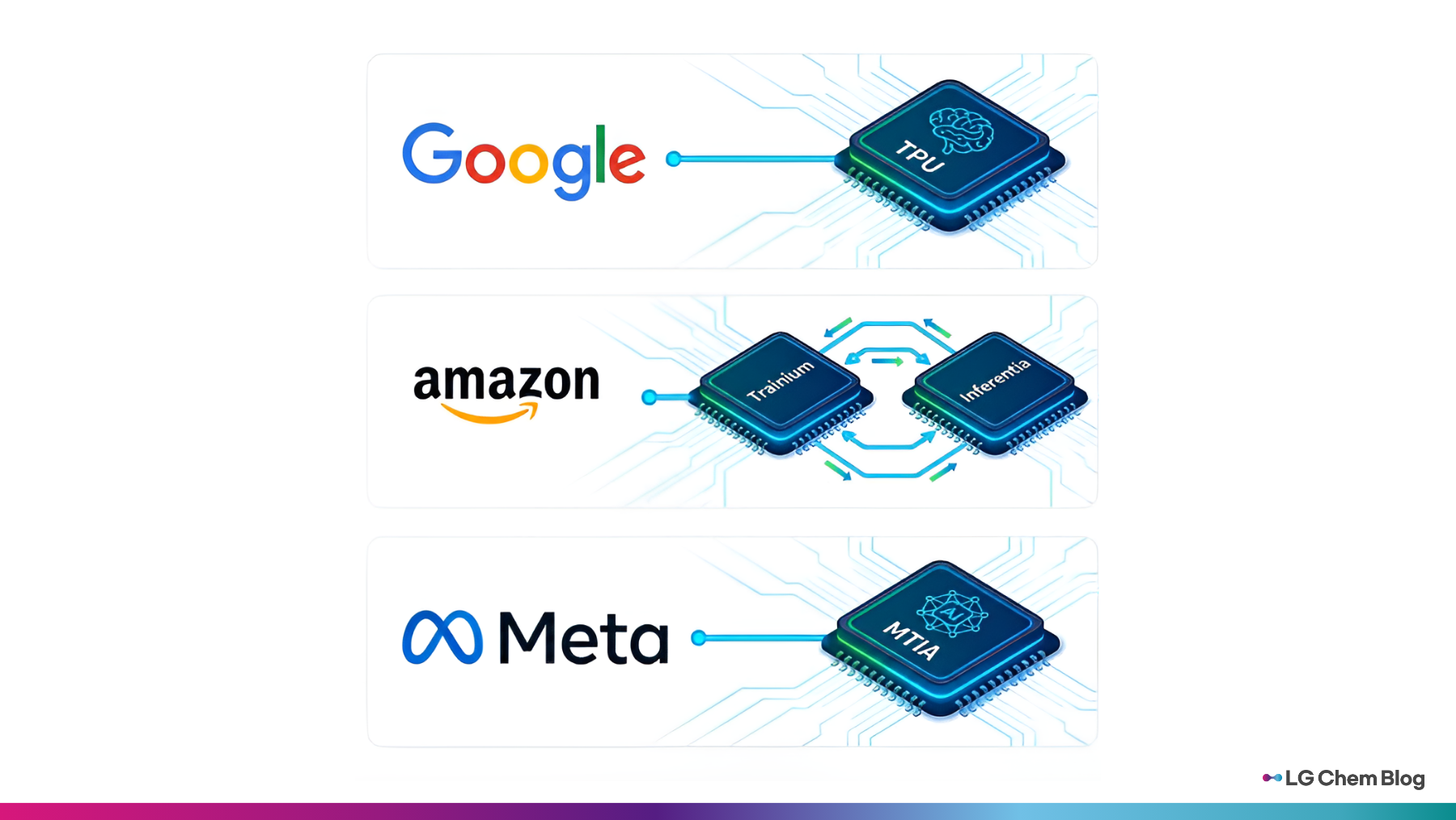
Why are companies outside the semiconductor industry starting to design their own chips?
As AI data centers grow larger, overall system performance, power efficiency, and operating costs become more important than the performance or price of any single chip. The companies that operate AI services know best which services they run and at what scale, which computations are repeated, and how data moves through their systems. Designing chips specifically for their own software and data centers can therefore offer significant advantages.
In the AI era, semiconductor companies are expanding into software and systems, while technology companies are becoming directly involved in chip design. As a result, the boundary between the two industries is rapidly blurring.
Why Has HBM Suddenly Become So Important in the AI Era?
Even the smartest person cannot work quickly if the information they need arrives too slowly. The same is true for AI chips.
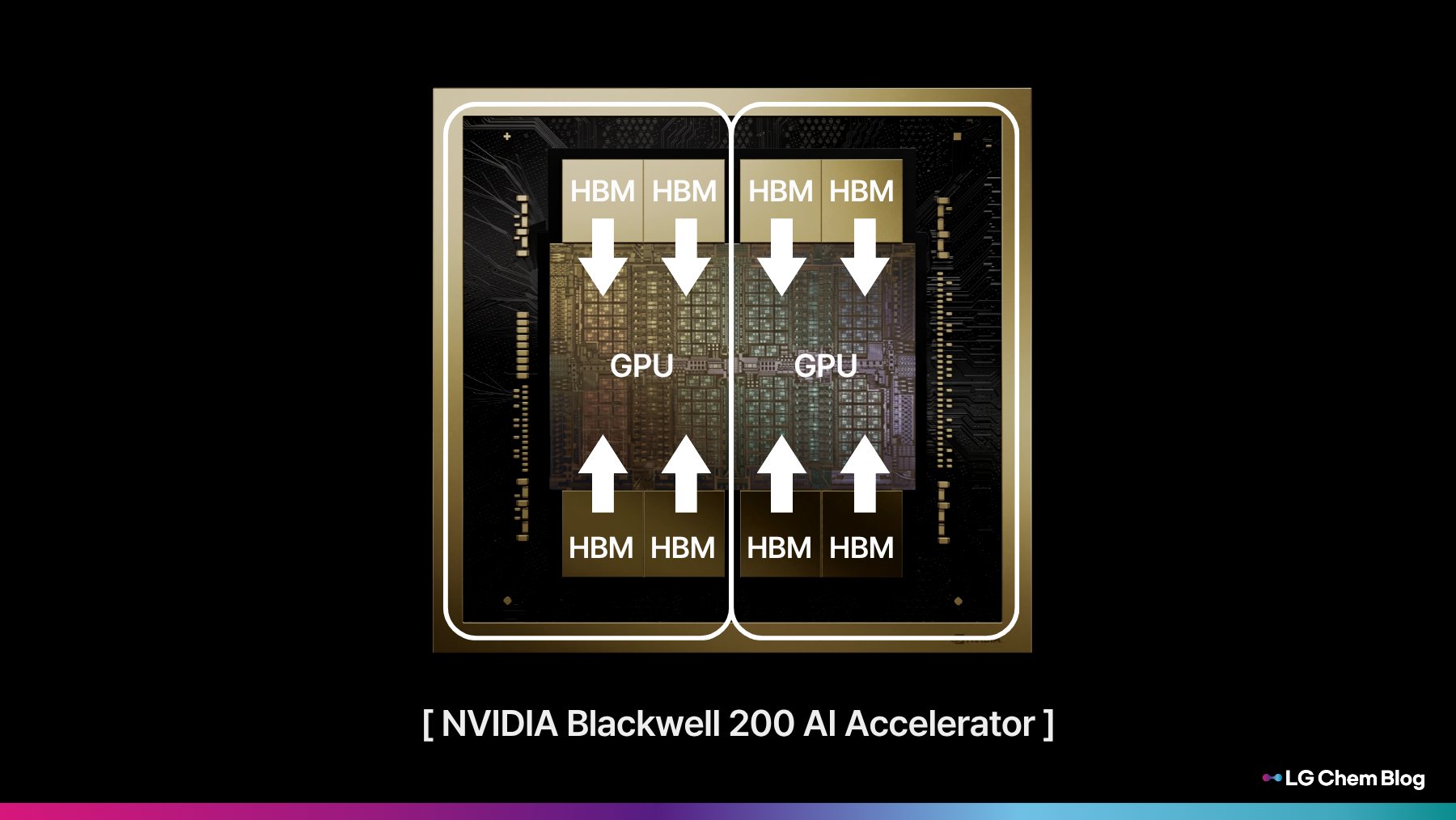
While CPUs once served as the brains of PCs, GPUs, which excel at large-scale parallel processing, have emerged as key chips in the AI era. The problem is that no matter how quickly GPU computing power advances, GPUs still have to wait for data if memory cannot keep up. This is known as the memory wall.
One important solution is high-bandwidth memory (HBM). HBM is a type of high-performance memory that stacks multiple memory chips vertically and uses wide data pathways to transfer large amounts of data quickly between the GPU and memory. In the AI era, how quickly data can be supplied for computation has become just as important as how quickly calculations can be performed. In the past, memory was often seen primarily as a component for storing data. In AI systems, however, memory bandwidth and capacity have become key factors in overall computing performance.
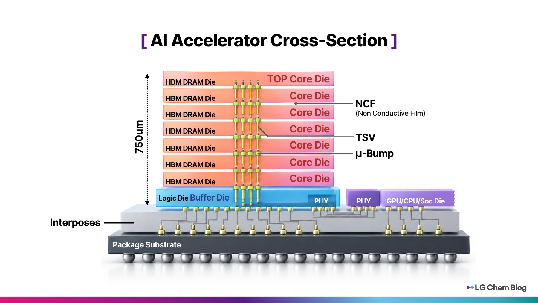
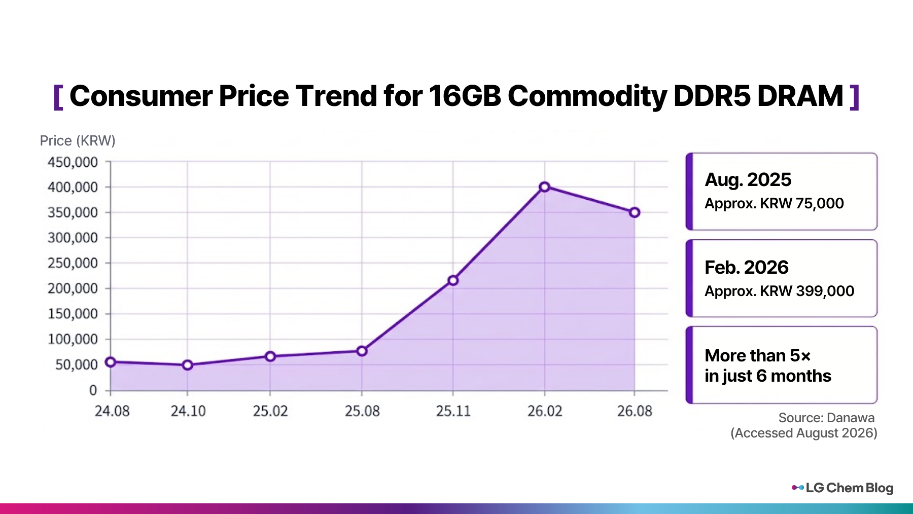
As demand for HBM surges, memory manufacturers are shifting more of their production resources toward it. HBM requires wider input/output (I/O) interfaces and through-silicon vias (TSVs) compared with conventional DRAM. Stacking, testing, and packaging multiple DRAM chips also require more wafers and manufacturing resources. As a result, expanding HBM production can reduce the manufacturing capacity available for conventional DRAM. Along with other factors, including demand, inventory levels, investment, and production shifts, this has also created significant upward pressure on prices in the broader memory market.
Why Has Semiconductor Packaging Become an Advanced Technology?
In the past, semiconductor packaging was often seen as little more than the final step in protecting finished chips and connecting them to external systems. But in the AI era, that has changed significantly. As GPUs become more powerful and HBM grows increasingly important, GPUs and multiple HBM stacks need to be connected as closely and efficiently as possible. For multiple chips to work together as a single system, engineers must consider the distance data travels between chips, communication speed, and power consumption. This is why advanced packaging has emerged as a key technology in determining AI chip performance.
This shift also signals a change in how semiconductor companies compete. In the past, the key question was, “Who can make the best chip?” Today, an increasingly important question is, “Who can best integrate multiple chips, memory, networking, and software into a single system?”
Does South Korea Have an Advantage in the AI Era?
The changes we have explored so far reveal a clear pattern. AI is not only increasing demand for semiconductors, but also changing who designs chips, where bottlenecks emerge, and how companies compete. Against this backdrop, South Korea has clear strengths. Led by Samsung Electronics and SK hynix, the country has world-class capabilities in memory semiconductors and holds an important position in the HBM market.
However, the picture looks different when we consider the entire AI semiconductor ecosystem. South Korea still faces gaps with global industry leaders in areas such as design of high-performance logic chips, including AI accelerators, core intellectual property (IP)* for CPUs and GPUs, electronic design automation (EDA), certain advanced manufacturing equipment, and software platforms. While the country has globally competitive capabilities in some areas of semiconductor materials, components, and equipment, its strengths vary significantly across the broader industry.
The question is no longer just “How well can we manufacture memory chips?” We also need to ask, “How many indispensable positions do we hold in the global semiconductor ecosystem?”
*IP (Intellectual Property): Proven circuit design assets used in semiconductor design.
So, what other indispensable roles should South Korea establish amid these major changes? New opportunities remain across the semiconductor ecosystem, from chip design, IP, and EDA to equipment, materials, and packaging.
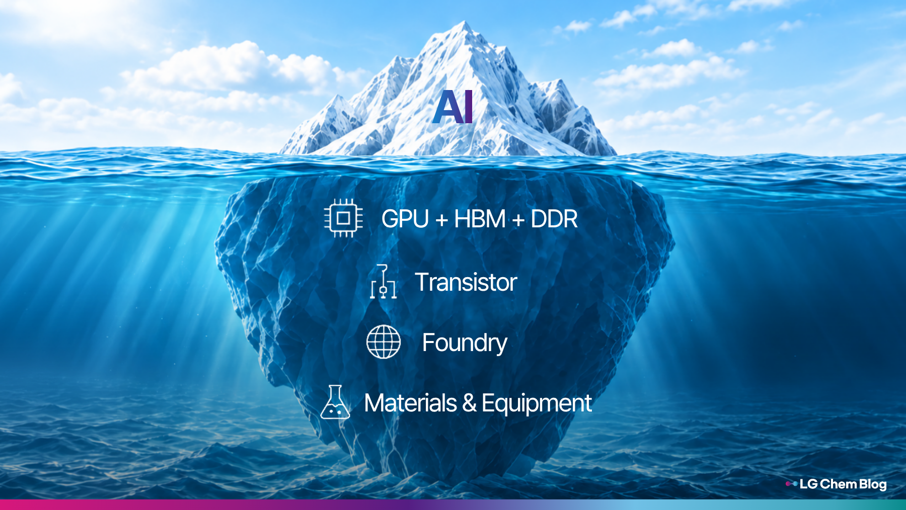
To find these opportunities, we need to look beyond the AI technologies we see today. We need to recognize the “invisible semiconductors” beneath the surface of the AI iceberg that make it all possible. In the next article, we will explore where the next key areas of competition in the semiconductor industry may emerge in the AI era.
About the Author
LG Chem Semiconductor Materials Insights Series
This series shares in depth knowledge and insights from LG Chem together with experts and opinion leaders in the field of semiconductor materials.
From changes in the semiconductor industry brought about by the AI era to advanced packaging technologies, next generation core materials, and the outlook for the future industrial ecosystem, the series will explore key developments shaping the semiconductor industry.
[🔍 More from the “Semiconductors Through Materials” Series]
Part 1) Why We Need to Look at the Semiconductors Behind AI
※ Some images in this content were generated using AI





There are no comments yet! Be the first to let us know your thoughts!